|
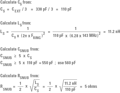
下面是从TI的网站找的,基本原理是差不多的。Snubber Circuit Design - Practical Tips Snubbers are used to limit switching transients and help lower EMI. - Measure the ring frequency at the top of the MOSFET switch node (SW) turn-off waveform. Solder a good quality COG or film type capacitor from the MOSFET SW node to GND, causing the ring frequency to be half of the original value. The effective capacitance at this node is 1/3 of the external capacitor value. The stray inductance is calculated using:

where CT is the total (effective plus external) capacitance. - In order to critically damp the ringing, double the size of the external cap. Use a series R calculated from:

where d is the damping factor, set to a value of 1. CS is the calculated effective capacitance at the SW node, not the external snubber capacitance. - Install the snubber resistor in the ground side of the RC circuit. If the ringing is not critically damped, the external capacitor value is too low. However, increasing this value may not be practical. Measure the positive and negative voltage spikes across the snubber resistor, which will be highest at the maximum input voltage. The power dissipated in the resistor is calculated by:

where VP and VN represent the positive and negative voltage spikes across the snubber resistor, and FSW is the switching frequency. This could be an unacceptably high amount of power dissipation. If so, a compromise between efficiency and damping may be required.
For parallel damping, the relationship is:


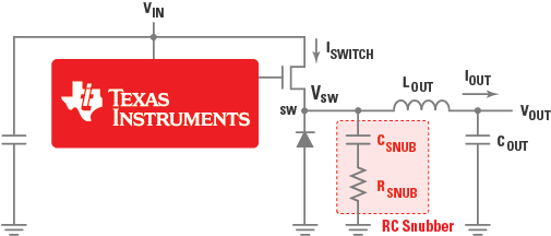
Buck Converter Snubber Circuit Design ExampleMeasure the switching signal at the MOSFET/inductor junction. You will see a voltage spike and ringing at the top of this signal. Let's say you measure a ring period of 7 ns, which represents 143 MHz. Solder a capacitor directly across the low side FET from the switch node to ground. Let's say 330 pF causes the period to double to 14 ns. Install RSNUB and CSNUB. Lets say at 40V input you measure Vpos = 40V and Vneg = 20V across the resistor. For 150 kHz operation:
|  [复制链接]


 发表于 2014-11-30 23:10:16

 很好 thanks
  楼主
楼主 谢谢老兄,RCD吸收确实是个头疼的问题,一不小心管子就死翘翘了。