|
|
TB6560 DATASHEET里有段话:
Turn on VDD. Then, when the VDD voltage has stabilized, turn on VMA/B.
Hold the control input pins Low while turning on VDD and VMA/B.
(All the control input pins are internally pulled down.)
After VDD and VMA/B completely stabilizes at the rated voltages, the RESET and ENABLE pins can be
set High. If this sequence is not properly followed, the IC may not operate correctly, or the IC and the
peripheral parts may be damaged.
大概意思是上电先上5V,再上VMA/B电压,5V和VMA/B上电时各输入引脚应该是低电平(网上找到的原理图大部分输入口常态置高),全部输入口芯片内部有下拉电阻。
在VDD和VMA/B电压稳定后,复位和使能引脚才能置高。如果这个上电顺序不正确,该芯片可能无法正常运行,或者会损坏芯片。
我在论坛里搜到这个帖子
http://www.ourdev.cn/bbs/bbs_content.jsp?bbs_sn=3468811&bbs_page_no=198&bbs_id=1000
先感谢仙猫提供的思路
改动后我画的图:
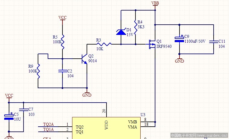
(原文件名:上电顺序.jpg)
问一下:
1、R5、R9阻值有没有问题?
2、当没有R9时,用公式:延时时间= -R*C*ln((E-V)/E) 算出9014基极从0V上升到0.6V的时间是1.28MS,现在有了R9,延时时间怎么确定?
3、复位脚用的是10K 10uF延时电路,这个电路能保证VMA/B上电时间比复位端早吗?
我用的VBB大概34V
PMOS DATASHEETourdev_614449HTNHX7.rar(文件大小:78K) (原文件名:IRF9540.rar) |
|


 发表于 2011-2-1 20:42:41
 楼主
楼主
