搜索
bottom↓
回复: 45

关于PSoC GPIO的应用讨论___问题不是这样的简单,已经发到CYPRESS请求帮助,结果和总结

[复制链接]

出0入0汤圆

发表于 2008-11-1 16:45:48 | 显示全部楼层 |阅读模式
没办法了,被阿莫当枪使了,就先“吐点血”,发本栏第一个在技术上做深入的讨论帖子吧(注意,CYPRESS站上没有的)。


GPIO是最基本的外围了,看似简单的东西,但PSoC的GPIO可不简单,如果不深入了解,使用起来一定会吃亏的。


PSoC的GPIO性能比AVR还强悍,可是使用起来却要非常注意。


从PSoC的手册上查到,PSoC的一个GPIO可以最大提供50mA输出电流,和容纳25mA的灌电流。


IMIO    Maximum Current into any Port Pin      -25   –   +50 mA

LU      Latch-up Current                        –   –   200 mA


典型的内部上拉和下拉电阻是5.6k。见下面的GPIO示意图:


 (原文件名:PSoC_GPIO.jpg) 


8个GPIO构成一个PORT,其中每一位GPIO,可以独立工作在8种工作方式下(厉害)。


每个POTR有4个8位寄存器控制,分别是:PRTxDR、DM2、DM1、DM0。PRTxDR是输出数据寄存器,而DM2-DM0是工作方式的设置。


!!!请仔细看图,容易出现问题的是:读GPIO时读到的不是PRTxDR寄存器的值,实际是引脚上的实际电平值!!!

!!!另外PSoC没有位操作,不能单独设置位,所以应用中非常容易出问题,而且不容易找到原因!!!


下面我逐步介绍如何正确使用GPIO的数字使用。


1。PSoC的外部引脚可以动态配置,如作为模拟信号的输入,或作为某个时钟信号的输入与内部某数字模块理解等。这给PCB设计走线提供了很多方便。但需要注意的是,某些用户模块,规定了与固定外部引脚的连接使用,因此系统设计过程中,要先把要使用的用户模块导入放置好,然后再确定剩下的引脚的使用,如控制LED指示等。不要上来就随便使用GPIO,进行硬件设计,这样可以防止多次改板。这是本人吃亏后得到的经验。


2。然后要确定你使用的GPIO应该是什么方式的。这里模拟输入方式6就不在讨论之列,因为此种方式与PRTxDR无关了,就是模拟高阻输入了。我们主要看数字应用。

    下面是方式表

DM2    DM0    DM1     Drive Mode             方式            PRTxDR=0       PRTxDR=1

 0      0      0     Resistive Pull Down       0             Resistive      Strong

 0      0      1     Strong Drive              1             Strong         Strong

 0      1      0     High Impedance            2             Hi-Z           Hi-Z           (数字高阻输入方式)

 0      1      1     Resistive Pull Up         3             Strong         Resistive

 1      0      0     Open Drain,Drives High    4             Hi-Z           Strong (Slow)

 1      0      1     Slow Strong Drive         5             Strong (Slow)  Strong (Slow)

 1      1      0     High Impedance Analog     6             Hi-Z           Hi-Z           (模拟高阻输入方式,不在讨论范围)

 1      1      1     Open Drain,Drives Low     7             Strong (Slow)  Hi-Z


   先要学会仔细看表,了解GPIO的工作方式。

   例如方式0,为下拉有效。注意它表示引脚输出0时(PRTxDR=0),内部是通过下拉电阻到0的。而当PRTxDR=1,则输出1高电平,可以提供大电流输出,而此时的内部下拉已经无效了(见上面示意图中的0)。

   另外,8种方式中有2种是纯输入方式,那么其它6种方式只能输出吗(当然这是没问题的),输入使用可以吗(见下面讨论)?


3。输出的使用。

   看似输出应用最简单,只要将输出那位的PRTxRD设置成0或1就可以了。实际不是!!,因为PSoC没有位操作,因此,需要进行8位的写操作(PSoC的缺点)。为了保证一位的改变,不影响其它的位,根据CYPRESS提供的资料,应该使用PRTxDR &= 0xfe 或 PRTxDR |= 0x01的方式(对第0位清另或置1),点击此处下载 ourdev_477999.pdf(文件大小:64K) (原文件名:user_interface___data_port_bit_manipulation_with_the_psoc_mcu___an2033_12.pdf) 

可是问题就出在这里。

   假定位1为输出,输出1,连接三极管的基极,驱动一个蜂鸣器。但由于三极管基极的嵌位(0.7v),实际引脚上的电压只有3v左右(考虑串入电阻后)。如果此时你要设置0位输出0,使用了PRTxDR &= 0xfe就非常可能出现问题了。

   PRTxDR &= 0xfe 相当于 PRTxDR = PRTxDR & 0xfe,这里要回读PRTxRD的值,但回读的值不是寄存器中的值,而是引脚的实际电平(见上面图中画圈部分)值!那么1位脚读到3V,很可能不是逻辑1,而是逻辑0!那么PRTxDR &= 0xfe执行后,0位到是输出0了,但1位也同时输出0了,而后面的则是不应该出现和一般估计不到的。

   解决办法是,在内存中建立一个变量比如PTRxRD_BUFF,为PRTxRD的副本,使用下面的方法对某位清0或置1。

   PRTxDR_BUFF &= 0xfe;

   PRTxDR = PRTxDR_BUFF; 

或:

   PRTxDR_BUFF |= 0x01;

   PRTxDR = PRTxDR_BUFF;

   好在PSoC内部的RAM还比较多,至少比51多。


4。数字输入使用。

   GPIO的8中方式中只有一种方式2,明确应用于数字输入,此时引脚为高阻输入方式。那么其它方式能不能作为输入使用,比如,外部接个按键,那么输入方式最好是带上拉电阻的,否则外部还需要多加上个电阻。

   实际上,方式3就是带内部上拉的(DM2/DM1/DM0=0/1/1,PRTxRD = 1),其本身完全可以作为输入引脚,外部接个按键。因为读PRTxRD是直接读的引脚电平,而不是寄存器的值。

   在具体使用中,更加要当心,原因还是由于上面第3点提到的,注意不要误改变PRTxRD寄存器的值。


总结:

   在硬件设计过程中,尽量把数字输入口集中在一个8位的PORT上,能不同输出的混用最好。

   为每个PORT的PRTxDR都在内存中建立一个副本。


================================================================

所谓的“吐血”,是指上面发生的情况都是我在做东西过程中碰到了,然后化时间找出原因,并找到解决的办法。在这里总结出来,没有保留的提供大家参考。

实际上,我碰到的问题还有许多,有一个问题至今还没得到CYPRESS的解答(发到官方站上的技术支持)。   


本贴被 machao 编辑过,最后修改时间:2008-11-30,12:16:58.

阿莫论坛20周年了!感谢大家的支持与爱护!!

月入3000的是反美的。收入3万是亲美的。收入30万是移民美国的。收入300万是取得绿卡后回国,教唆那些3000来反美的!

出0入0汤圆

发表于 2008-11-4 10:19:25 | 显示全部楼层
学习了

出0入0汤圆

发表于 2008-11-6 22:55:37 | 显示全部楼层
呵呵,它不支持RRW(读-修改-写),不知道是不是可以这样理解。

出0入0汤圆

 楼主| 发表于 2008-11-17 16:42:40 | 显示全部楼层
我已经发到CY官方站询问了。不知道他们的答复是什么,或许我的水平不够,还没吃透PSoC的GPIO操作。

出0入0汤圆

发表于 2008-11-17 10:49:47 | 显示全部楼层
马老师的解决方案"为每个PORT的PRTxDR都在内存中建立一个副本。"

有一点要注意:

  例如如下代码(为了更好地说明问题,使用汇编)

               mov A,[PRT0DR_Copy]    ; 1

               or  A,01h              ; 2

               mov [PRT0DR_Copy],A    ; 3

               mov reg[PRT0DR],A      ; 4

   当代码执行完1,还没有执行4的时候(PC指针在2~3时).如果来了中断,并且在中断中也操作了PRT0DR.可能会出现PRT0DR被非法修改的可能.


   解决方法: AND   F,feh

             ;上面的代码

             OR    F,01h

出0入0汤圆

 楼主| 发表于 2008-11-17 16:29:58 | 显示全部楼层
楼上,你能确定吗?是否CY也是这样认定的?


那么PSoC的问题严重了,只能自己从头写代码,那些用户模块还敢使用吗?

出0入0汤圆

发表于 2008-11-17 15:49:18 | 显示全部楼层
1.等号后PRT0DR的值是引脚的实际电平,这也正是CY的GPIO存在的隐患.

2.实际引脚电平通过DM[2:0]=110b的2输入施密特或门到达内部总线,再通过上图Read PRTxDR(右上打黑框部分)读指令产生的允许脉冲到达Data Bus.

3.直接使用PRT0DR就是读取引脚的实际电平.汇编指令之一: mov A,reg[PRT0DR] C代码之一: xx = PRT0DR;

出0入0汤圆

 楼主| 发表于 2008-11-17 15:28:01 | 显示全部楼层
to 【5楼】 leon101010 ARC的蜈蚣:


看来您对PSoC还是非常了解的,能解释下面的问题吗?


PRT0DR &= 0xBF 实际就是 PRT0DR = PRT0DR & 0xBF 吧(汇编为 AND REG[PRT0DT],0xBF)。


那么等号后PRT0DR的值是什么?是PRT0DR寄存器的值,还是PRT0DR引脚的实际电平?如何与上面的图对应起来?


另外,如何读PRT0DR引脚上的实际电平?汇编和C如何编写?   

出0入0汤圆

 楼主| 发表于 2008-11-17 12:26:08 | 显示全部楼层
这确实是个问题。因为PSoC提供的用户模块中(不仅仅是中断)都可能直接改变PRTxDR的,而副本是不变的。


看来建立副本也不是万全之计,PSoC的GPIO有很大的问题。

出0入0汤圆

发表于 2008-11-30 20:45:40 | 显示全部楼层
PSoC是什么东西我都不知道

不过这个一定得留心了


上次看AVR手册的时候一句:

 (原文件名:AVR_DDR.jpg) 

思索了半天


细节,细心.学习

出0入0汤圆

 楼主| 发表于 2008-11-30 20:43:34 | 显示全部楼层
楼上正确,使用影子寄存器只是一种补救的措施,不是万能的,根本在于硬件结构上不是很完善。


所以说每个厂家的MCU都有自己的优点,也有不足的地方。

出0入0汤圆

发表于 2008-11-30 17:57:31 | 显示全部楼层
虽然我没用过PSoC,但是也说说我的想法

影子寄存器和引脚没法同时访问,所以可能会出现修改完一个,修改另一个之前被中断,而中断服务程序也要访问同一组引脚,可能会造成引脚状态和影子寄存器的破坏,所以,若对可靠性要求比较高的话,操作引脚和影子寄存器时应关闭中断或采用一定的写保护措施

例如增加一个影子寄存器保护位

访问引脚时先开启保护位,防止被中断程序无意修改,然后访问影子寄存器和引脚,完成后关闭保护位

但这种方法可能会阻塞中断服务程序访问引脚,解决这个又需要一大堆操作……

如果在访问影子寄存器和引脚时关闭中断,则可能导致重要中断的丢失或者延误……

总之麻烦


还有一个是要在系统初始化时要对影子寄存器赋初值,因为影子寄存器可能位于内存中,在复位或者短时掉电时可能并没有被清除,重新启动时可能会干扰软件的访问

本贴被 h2feo4 编辑过,最后修改时间:2008-11-30,18:00:05.

出0入0汤圆

 楼主| 发表于 2008-11-30 17:42:00 | 显示全部楼层
看来AVR的GPIO还是不错的,没有这样的麻烦。它要读I/O口的话,是PIN寄存器,与PORT寄存器分开的,不会出现这样的问题。

出0入0汤圆

发表于 2008-11-30 14:08:51 | 显示全部楼层
【28楼】 machao :


呵呵,我用PIC单片机也有影子寄存器的技巧的,比如IO的读-改-写的问题,如果IO的负载较重,读回来的值可能不是稍早前写入的值,因此会出问题。《PIC单片机入门与实战》张明峰 编著 这本书的一些章节也讨论了影子寄存器的用法问题,借楼主宝贴推荐一下。

出0入0汤圆

 楼主| 发表于 2008-11-30 12:00:38 | 显示全部楼层
我查到了更多的资料,实际上CY已经知道这个现象,在开发平台中有专门的文献介绍如何使用“影子”寄存器:点击此处下载 ourdev_522716.pdf(文件大小:42K) (原文件名:ShadowRegs.pdf) 。


但主要的是,PSoC提供的用户模块基本上都没有使用ShadowRegs,所以在自己的实际系统的设计和调试中,一定要注意,碰到一些奇怪的情况,先考虑是否是由于I/O的这个特点而造成的。


==========================================================

以下摘自ShadowRegs.pdf 


Theory of Operation

Data written to a port data register may differ from data read from the port data register because the read data represents actual pin voltages while the written data controls the pin output setting (transistor switching). This difference between the read and written data introduces the risk of inadvertently corrupting a pin's output setting when performing a logical operation directly on the port data register to affect the setting of a different pin sharing the same port. This situation commonly occurs with pins operating in resistively pulled-up/pulled-down, or open drain drive modes.


Example

An application uses P0[0] as a sourcing LED output, and P0[1] as a pulled-up input for a normally open switch connected to ground. After setting the drive mode registers for port 0, the firmware initializes the LED to off and enables the input with the following C statement.

PRT0DR = 0x02; Without a shadow, register, the firmware toggles the LED by the following C statement.

PRT0DR ^= 0x01;

On the initial LED toggle operation, the value read from PRT0DR is 0x00 if the switch is closed, and 0x02 if the switch is open. Performing the XOR operation to toggle the LED results in 0x01 (0x00 XOR 0x01) if the switch is closed but 0x03 (0x02 XOR 0x01) if the switch is open when the initial toggle occurs.

Toggling the LED when the switch is closed causes P0[1] to be driven to 0V internally. When the switch is opened, the value read from PRT0DR is still 0x01 because the voltage on P0[1] is still 0V. The switch input has been inadvertently disabled.


The solution is to always manipulate the shadow register first, then copy the shadow register value into the port data register. The following C statements initialize the LED output and the switch input.

Port0_Data_Shade = 0x02;

PRT0DR = Port0_Data_Shade;


The following code toggles the LED without affecting the switch input

Port0_Data_Shade ^= 0x01;

PRT0DR = Port0_Data_Shade;

Regardless of whether the switch is open or closed, 0x03 (0x02 XOR 0x01) is written to the port data register on the initial toggle operation because the logical operation was performed using the shadow

register (0x02 regardless of whether button is open or closed) as input rather than the port data register (0x00 when the switch is closed, and 0x02 when the switch is open)


本贴被 machao 编辑过,最后修改时间:2008-11-30,12:13:10.

出0入0汤圆

发表于 2009-1-21 18:02:24 | 显示全部楼层
CY连软仿真都没有

出0入0汤圆

 楼主| 发表于 2008-12-1 23:15:19 | 显示全部楼层
AVR也可以,51也可以的。这个不是优点。


在AVR、51、PIC中,只有AVR的I/O可以直接(真正)方便的实现“读-改-写”操作。根本不需要使用“影子”寄存器。AVR的I/O比51、PIC的能力都强,使用更加方便。

出0入0汤圆

发表于 2008-12-1 21:53:34 | 显示全部楼层
【30楼】 machao


呵呵,PIC这种设置也不是一无是处的,可以有许多非常用法,比如用单IO测量外部电容大小,或负载情况一类的奇怪应用,不用再增加其它芯片。

出0入0汤圆

发表于 2009-1-2 23:19:55 | 显示全部楼层
上拉 上拉 再上拉


51上我也碰过几回非的上拉

出0入0汤圆

发表于 2008-11-1 19:08:08 | 显示全部楼层
顶了先    慢慢看 谢谢马老师 

出0入0汤圆

发表于 2008-11-1 17:18:10 | 显示全部楼层


 (原文件名:ourdev_477958.jpg) 

方便观看。

出0入0汤圆

发表于 2008-11-30 10:21:22 | 显示全部楼层
恩,我用psoc做个很简单的数字并口输出,搞了半天还弄不懂...

出0入0汤圆

发表于 2008-11-29 10:37:05 | 显示全部楼层
问题越讨论越清楚。学习了

出0入0汤圆

发表于 2008-11-21 13:23:59 | 显示全部楼层
严重支持马老师!

出0入0汤圆

 楼主| 发表于 2008-11-21 12:03:49 | 显示全部楼层
特点:

1。模拟模块,可以实现很多模拟、模拟数字混合的使用。这是其它所不具备的。

2。资源、引脚的可配置,利用率高。

3。提供大量的用户模块使用,可以使用户尽可能的跳过低层。

4。带USB接口功能


以上是重要的特点,这些特点体现出了目前技术的一些新的发展和变化。本身芯片的价格不是太贵,因此我现在玩它,是学习、了解和做技术储备。


PSoC目前还不是非常完善,我想CY也会不断的做改进的。我不是让大家放弃AVR、51、PIC,是希望大家了解点新的东西。只有你了解它的特点后,或许对设计有些系统和产品有帮助。


比如,在本栏中我的一个帖子,采用PSoC设计的触摸式的用户界面控制盘,如果使用普通的AVR、51等8位系统来实现就比较困难了。

本贴被 machao 编辑过,最后修改时间:2008-11-21,12:41:36.

出0入0汤圆

发表于 2008-11-21 10:58:06 | 显示全部楼层
马老师,这个IC成本很低吗??感觉跟AVR比起来都没有什么优势,更不要说NEC、瑞萨了

跟台湾IC比起来,估计更惨


而且从性能上、稳定性上说,AVR、NEC、瑞萨都不会比它差


您当初选择这款IC的出发点是什么呢??


我个人感觉是趁早放弃转型比较合适

出0入0汤圆

 楼主| 发表于 2008-11-19 00:09:48 | 显示全部楼层
在21楼我把与CY官方站支持工程师Sachin关于GPIO的讨论全部贴上了,供大家参考。


使我不明白是,到底是CY已经知道PSoC的GPIO有弱点而掩掩盖盖、吱吱唔晤呢,还是由于我的E文太差,他们看不懂我说的问题。不过费了半天的劲,他们总算给出了明确的答复:


1。No, PSoC do not have commands for bit operations. Whenever you read the port, you can read pin value only. You will need to use one temporary variable to keep track of written data. 


2。Yeah, you are right. It is advised to keep High-Z pins to be tied at some fixed level externally. There is no other solution.


因此,PSoC的GPIO有缺点是肯定的了,大家使用中千万注意!

出0入0汤圆

 楼主| 发表于 2008-11-18 20:44:11 | 显示全部楼层
与CY 支持工程师的对话(时间顺序从下往上,目前还没有CLOSE):


=====Cypress Response   Sachin Gupta | 11/18/2008 07:37 AM | Web 

Yeah, you are right. It is advised to keep High-Z pins to be tied at some fixed level externally. There is no other solution.  //!!!(2)


Best regards, 

Sachin


===== Customer Comment   Ma Chao | 11/18/2008 07:30 AM | Web 

But you have not got it correctly. 


Not only PRT0DR |=0x01 but also PRT0DR &= 0xFE is only OK for P0[0] . BUT MAY BE CHANGGE OTHER VALUES OF PRT0DR REGISTER THAN PRT0DR[0]!!! Because the other pins status is not the same as the values of port register. 


===== Cypress Response   Sachin Gupta | 11/18/2008 07:23 AM | Web 

your reset pin may be at any logic as you are driving the line to High-Z(means unconnected). So it may be at any logic according to noise. 


===== Cypress Response   Sachin Gupta | 11/18/2008 07:18 AM | Web 

yeah! now you have got it correctly. 


===== Customer Comment   Ma Chao | 11/18/2008 07:07 AM | Web 

Apart from that when you want make P0[0] high, then you write: 


PRT0DR |=0x01; 


This instruction will effect on P0[0] not other pins. Because you are performing the OR operation. If you OR any pin which '0' then pin value will not change. 


If you want to clear the P0[0], then you use 


PRT0DR &= 0xFE; 


Now P0[0] will be cleared. But other pins will not be effected. As performing AND operation with '1' will not effect the original pin status of pins other than P0[0]. 


The key is when change P0[0], I WILL NOT CHANGE OTHER VALUE OF PORT0 REG THAN P0[0]. the other pin status may be DIFF from REG! 


===== Customer Comment   Ma Chao | 11/18/2008 06:50 AM | Web 

LCD only use 7 pins, but PORT 2 have 8 pins, 


OK. Let us talk abour LED UM ,for example, use PORT0.0 for LED, and I also use PORT0.1 for controling a RESET pin of other chip. 


beging I will set my RESET pin HZ (PORT0.1 works as Open Drain,Drives Low ): 


PRT0DR |=0x02; // SET port0.1 PIN High-Z 


after that it comes your LED UM 


PRT0DR |= 0x01; // turn on LED 


OK, The LED UM must frist read PRT0DR, but is PIN value not REG. At this time wath value is PORT0.1 that is High-Z state? Is "1" or "0"? 


MAYBE "0"!! THEN PRT0DR = 0x00(value of pins) | 0x01, Yes, the LED is turned on, but what about my RESET pin? IS "1" OR "0"? 


===== Cypress Response   Sachin Gupta | 11/18/2008 06:14 AM | Web 

You are not supposed to use same pins for both purpose. For example if you are using port 2 for LCD then you should not use the port for other things. 


Apart from that when you want make P0[0] high, then you write: 


PRT0DR |=0x01; 


This instruction will effect on P0[0] not other pins. Because you are performing the OR operation. If you OR any pin which '0' then pin value will not change. 


If you want to clear the P0[0], then you use 


PRT0DR &= 0xFE; 


Now P0[0] will be cleared. But other pins will not be effected. As performing AND operation with '1' will not effect the original pin status of pins other than P0[0]. 


Let me know if it clears your doubt. 


Best regards, 

Sachin 


===== Customer Comment   Ma Chao | 11/18/2008 06:02 AM | Web 

Thanks very mush for your kindly support service. Are you speaking chinese,? My english speaking is poor. So I like type same words to you. 


Yes, your LCD used pin is right, LCD no problem. But the LCD UM may changed the Other PIN VALUE that I used at the same port as the LCD! 


In API like for LCD, we do not need to read the data which I have written to that port (you must read port, but this port have other pin that LCD no used be using by I ). 


So, I do not need to keep any temp variable . I just need to read input pins (this pins also include my used pin, not the PINS that only LCD used) and that can I do ass I told earlier (so my pins also be chenged! And I had not known! ). 


===== Cypress Response   Sachin Gupta | 11/18/2008 05:21 AM | Web 

In API like for LCD, we do not need to read the data which I have written to that port. So, I do not need to keep any temp variable. I just need to read input pins and that can I do ass I told earlier. 


If you still have any doubt regarding this issue, then please give me your contact number. I will give a call to you. 


Best regards, 

Sachin


===== Customer Comment   Ma Chao | 11/18/2008 05:18 AM | Web 

LED,LCD......many user module need change the port pin. Do they use temporary variable? When a pin used by my code and a pin used by LED MU are at the same port, what can I do? Using the temporary variable?


===== Cypress Response   Sachin Gupta | 11/18/2008 05:01 AM | Web 

which user module you are talking about? 


Best regards, 

Sachin


===== Customer Comment   Ma Chao | 11/18/2008 04:37 AM | Web 

ok. 

But what about the USER MU? is it using the temporary variable? And how I use the temporary variable in my code with USER UM togather? 


===== Cypress Response   Sachin Gupta | 11/18/2008 03:33 AM | Web 

I gave you one example about strong and High-Z mode. If a pin is configures for output, then if you write 


PRT0DR = ---; 


Then the pin status will be the same what you write on that. 


No, PSoC do not have commands for bit operations. Whenever you read the port, you can read pin value only. You will need to use one temporary variable to keep track of written data.    //!!!!(1)


Let me know if I may go ahead and close this case. 


Best regards, 

Sachin


===== Customer Comment   Ma Chao | 11/18/2008 03:00 AM | Web 

so problem will come. if do this: 


PRT0DR |= 0x01; // works as Open Drain,Drives Low, only set port.0 High-Z 

PRT0DR |= 0x02; // only set port.1 high 


as you sey: "your pin P0[0] will become '1' for sure. But if you keep the mode as High-Z then it will not effect the pin status." . after the second sentens the port.0 PIN maybe not be High-Z! 


I will say ,the PSoC have not the bit oprations and must use READ-MODIFY-WRITE to change a bit. As this time the beste way is read port register not PIN value! 


I will knew how can read the value of port register? 


===== Cypress Response   Sachin Gupta | 11/18/2008 12:31 AM | Web 

It depends upon the drive mode which you have select for a particular pin. If you select port 0 as Strong and then write 


PRT0DR |= 0x01; //only set port.0 high, 


your pin P0[0] will become '1' for sure. But if you keep the mode as High-Z then it will not effect the pin status. 


Let me know if it answers your question. 


Best regards, 

Sachin 


===== Customer Comment   Ma Chao | 11/17/2008 11:50 PM | Web 

In same actual situation, the PIN value is not the same as port regist. At this time, when you change one port bit maybe another port bit also be changed. For example: 


PRT0DR |= 0x01; //only set port.0 high 

PRT0DR |= 0x02; //only set port.1 high 


after the first sentens the PRT0DR register is 0x01, but the port.0 PIN maybe not be high. So the second sentens may not only set port.1 high (needed) but also clear the port.0(not needed!) 


===== Cypress Response   Sachin Gupta | 11/17/2008 07:16 PM | Web 

Dear Ma Chao, 


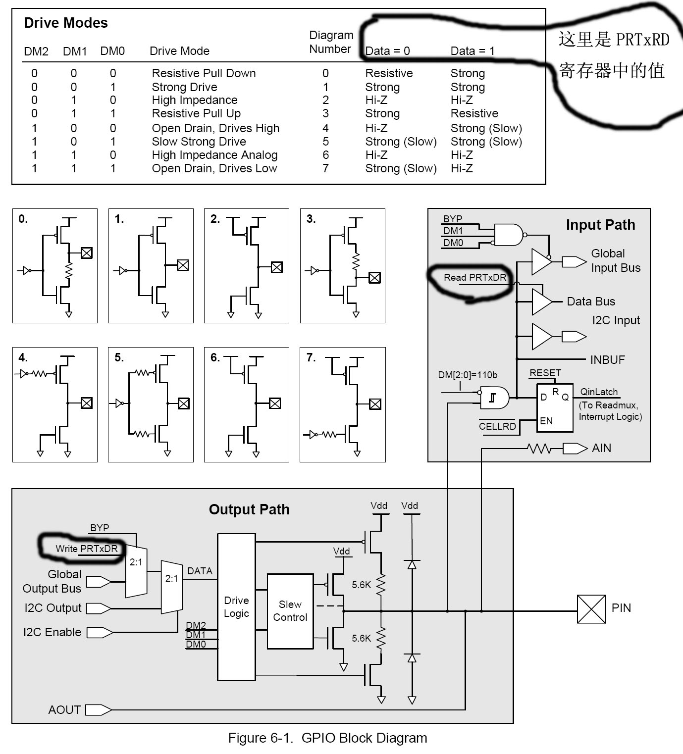
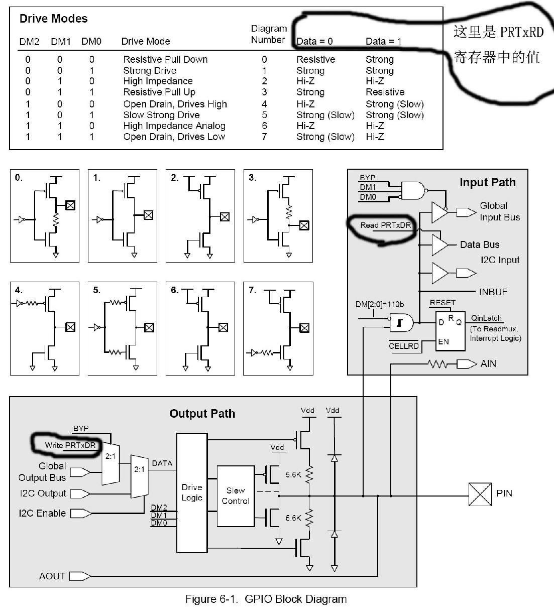
I would like to give you a broad idea about ports. Basically ports uses that shadow register. When you write anything on port, that is written in the PRTxDR write register: 


PRT0DR = ------; 

This is the internal register. 


When you read the port: 


------ = PRT0DR; 

This is port pin itself. 


Let me know if it clears your doubt. 


Best regards, 

Sachin


===== Customer Comment   Ma Chao | 11/17/2008 10:24 AM | Web 

Thanks for your response. 


Thinking of that the PIN value maybe not same as PRT0DR REG, when you change one port bit maybe another port bit also be changed? 


===== Cypress Response   Sachin Gupta | 11/17/2008 02:08 AM | Web 

Dear Ma Chao, 


Yes, PRT0DR &= 0xBF is same as PRT0DR = PRT0DR & 0xBF. 


These instructions read the pin status, perform & 0xBF and then output it on PRT0DR itself. 


PRT0DR on the right hand side is the actual PIN value. 


To read PRT0DR PIN value use: 


variable = PRT0DR; //variable is any byte size variable 


Let me know if it answers your questions. 


Best regards, 

Sachin

本贴被 machao 编辑过,最后修改时间:2008-11-19,00:11:38.

出0入0汤圆

发表于 2008-11-18 16:36:58 | 显示全部楼层
马潮老师很负责!强烈支持这样的老师!

出0入0汤圆

发表于 2008-11-18 15:56:52 | 显示全部楼层
嚴重關注

出0入0汤圆

 楼主| 发表于 2008-11-18 14:52:57 | 显示全部楼层
注意正确理解和使用PSoC的GPIO,不是那么简单,要多想想。


在实际情况中,由于某些原因,如干扰、所接器件特性的不同、硬件设计考虑不周等,都可能会造成PORT寄存器中的值与实际引脚的电平不同。


作为GPIO的输出,由于PSoC没有位操作,所以只能采用整个寄存器读-改-写的方式。但在这时,我们真正需要的,也只是需要PORT寄存器中的值,而不是PIN上的值。这样才能确定的保证改变1位并同时不影响其它位的输出。


但PSoC好象没有回读PORT寄存器的功能,而是用PIN的实际电平来代替,因此不了解的话,调试系统肯定费事的。

比如由于硬件设计的不合理,系统在调试中出现了问题。那么你将如何找到真正的原因,确定是硬件上的问题而去修改呢?当你知道PSoC的GPIO有这样的特点的话,可能就会很快找到根源去改硬件了,如果不知道,那就抓瞎吧。


使用镜象寄存器或影子寄存器是一种补救的措施,但当系统中使用了PSoC的用户模块后,此办法也会出问题的。因为PSoC的用户模块也可能会改变GPIO的输出,可是它们并没有采用镜象寄存器或影子寄存器。


在PSoC的GPIO结构图中,它使用了4个寄存器来控制一个8位的IO口,提供了8种工作方式,有内部上拉、下拉,高阻等许多特性,其目的就是让人使用方便,减低成本。


可是,最简单的挂一个按键,也必须使用外部加上拉电阻,否则就给你难看,这只能说是GPIO的一个不足了。


事情的起因就是所指导的学生,简单挂了一个按键,没有外加上拉,可是发现按键响应就是乱套的,我开始还说他,怎么连个按键也搞不定。然后自己做测试,才发现问题。

本贴被 machao 编辑过,最后修改时间:2008-11-18,15:03:43.

出0入0汤圆

发表于 2008-11-17 23:11:37 | 显示全部楼层
嗯,看来还是用AVR比较实际


论坛推广的NEC也不错,就是自带的编译器有些郁闷


正在学习IAR For NEC

出0入0汤圆

 楼主| 发表于 2008-11-17 22:06:58 | 显示全部楼层
下面是CY的答复,的确是存在一定的隐患。


Yes, PRT0DR &= 0xBF is same as PRT0DR = PRT0DR & 0xBF. 


These instructions read the pin status, perform & 0xBF and then output it on PRT0DR itself. 


PRT0DR on the right hand side is the actual PIN value. 


To read PRT0DR PIN value use: 


variable = PRT0DR; //variable is any byte size variable 


Let me know if it answers your questions. 


Best regards, 


=====================================

请见后面的分析和总结

本贴被 machao 编辑过,最后修改时间:2008-11-18,14:54:19.

出0入0汤圆

发表于 2008-11-17 19:58:54 | 显示全部楼层
学习了。。。

出0入0汤圆

 楼主| 发表于 2008-11-17 17:27:51 | 显示全部楼层
51有位操作,这个区别太大了。至少别的东西不会搞乱你的控制。你只要注意先输出“1”,再读就可以了,而且位操作,问题不大。


另外PIC、AVR都改进了I/O,实现了真正的双向功能,可PSoC做的比51还差?

出0入0汤圆

发表于 2008-11-17 17:16:58 | 显示全部楼层
"或许我的水平不够,还没吃透PSoC的GPIO操作"马老师谦虚了.


其实这个问题并不是只有CY才有,当初51就有同样的问题.所有IO口没有双缓存的芯片都有此问题.

出0入0汤圆

发表于 2008-11-17 16:54:59 | 显示全部楼层
哎,我连他的图形界面都还没有搞清楚,何论代码....

出0入0汤圆

发表于 2008-11-17 16:51:55 | 显示全部楼层
 我在实际使用中验证了上述问题,可以非常肯定.


我解决的方法:

 1.在配置中只适用DM=001;010;101;110这4中配置,并且输出口负载不能太重.

 2.如果一定要使用其他配置,只能避免在API中使用相同口或自己定义API;用户程序中关中断.

本贴被 leon101010 编辑过,最后修改时间:2008-11-17,16:59:10.

出0入0汤圆

发表于 2009-2-25 13:39:35 | 显示全部楼层
学习了

出0入0汤圆

发表于 2009-4-11 10:37:11 | 显示全部楼层
前几天使用时就有使用影子寄存器的想法,但是想到改写用户模块,真是头都大了,如果cypress出C代码的用户模块,而且可以重新定义修改(好像是在说开源)就好一些了,在汇编里改写工作量太大了(主要是效率低)。有没有cypress的工作人员看这个帖子啊?用户模块开放继承功能啊,是很需要使用提供的用户模块,但很多太单调了,多留一些接口给使用者啊,强烈建议!

出0入0汤圆

发表于 2009-12-15 11:37:53 | 显示全部楼层
强帖!先看后思,暂且记号。

出0入0汤圆

发表于 2010-7-19 18:47:38 | 显示全部楼层
回复【37楼】huang_hzl  
------------------------------------------------------------------
自己不也会买啊,都是模块化的,基本不用写程序,用什么仿真器啊?

出0入0汤圆

发表于 2011-6-14 21:43:36 | 显示全部楼层
mark

出0入0汤圆

发表于 2012-4-12 21:52:39 | 显示全部楼层
郁闷了3天后,终于研究出和上面相同的结果,baidu 一下,就看到楼主了,原来不是我一个人郁闷。

出0入0汤圆

发表于 2016-3-31 21:07:09 | 显示全部楼层
今天公司被迫改好多年的CY8C27443的代码 头都大!搞了一天的端口输入 监测端口高低变化 就是不行!痛苦。

出0入0汤圆

发表于 2016-3-31 21:10:05 | 显示全部楼层
if(PRT1DR ==0)
{
   char i=0;
}

我吧 PRT1DR  用电线短路到地,反映都没有。怎回事啊!?
回帖提示: 反政府言论将被立即封锁ID 在按“提交”前,请自问一下:我这样表达会给举报吗,会给自己惹麻烦吗? 另外:尽量不要使用Mark、顶等没有意义的回复。不得大量使用大字体和彩色字。【本论坛不允许直接上传手机拍摄图片,浪费大家下载带宽和论坛服务器空间,请压缩后(图片小于1兆)才上传。压缩方法可以在微信里面发给自己(不要勾选“原图),然后下载,就能得到压缩后的图片】。另外,手机版只能上传图片,要上传附件需要切换到电脑版(不需要使用电脑,手机上切换到电脑版就行,页面底部)。
您需要登录后才可以回帖 登录 | 注册

本版积分规则

手机版|Archiver|amobbs.com 阿莫电子技术论坛 ( 粤ICP备2022115958号, 版权所有:东莞阿莫电子贸易商行 创办于2004年 (公安交互式论坛备案:44190002001997 ) )

GMT+8, 2024-4-27 03:47

© Since 2004 www.amobbs.com, 原www.ourdev.cn, 原www.ouravr.com

快速回复 返回顶部 返回列表