|
|

楼主 |
发表于 2009-6-22 20:33:40
|
显示全部楼层
来源于:http://www.alternatezone.com/electronics/hsfg.htm
Low Cost 20MHz Function Generator :
=====================================
By David L. Jones
I thought that I had a relatively well equipped work bench up until a while
ago when I wanted to test some op-amp circuits for a new design. They needed
to work at several megahertz, and it would have been nice to test them at
over 10MHz. However, it all soon came to a halt when I remembered that both
of my function generators were only capable of a little over 1MHz. I did have
access to some expensive commercial digitally synthesised function generators
capable of over 10MHz, but I wanted a simple and low cost one for my own
bench !.
Want being the mother of invention, I put my current design aside for a
while (as usual!) and decided that I needed to build a high speed function
generator.
The first thing I did was to look for any previous function generator
projects that meet my requirements. The only one that catered for frequencies
in the MHz region was the digitally synthesised designed published in the
April 93 edition of EA. Whilst it did handle the frequency I needed, I wanted
something with real "KNOB'S" that could be easily adjusted.
The design was starting to look terribly complicated when along came the
MAX038 chip from Maxim in the United States. A complete 20MHz
sine/square/triangle function generator in a single chip !.
While it is possible to build a complete function generator using just the
MAX038 and a few capacitors and resistors, I found that it needed just a
little bit more circuitry to make it into a fully fledged function generator
design.
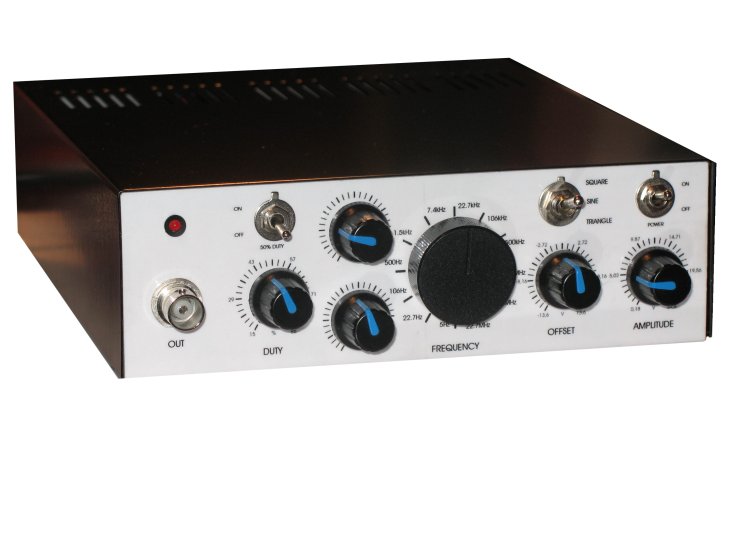
The final design described here is capable of producing sine, square,
triangle, and TTL level waveforms at up to and beyond 20MHz. See the
accompanying table for full specifications. Normally, an analog function
generator capable of this frequency would be very expensive and very complex.
But as you can see, this entire design consists of little more than three
IC's !.
Please note, this project has been designed for the highest possible
frequency coverage, and NOT for the lowest possible distortion level. With a
sine wave harmonic distortion of greater than 1%, it is not suited for
precision audio applications. But it should be fine for general audio use
however.
The MAX038 was originally quite hard to obtain in Australia, but it is now
stocked by RS Components and is quite readily obtainable. The performance of
the MAX038 does not come cheaply at almost $50 for the chip, however
considering the specifications of the device, it is the lowest cost way to
get a function generator in this frequency range.
To keep the cost of the unit to the absolute minimum, it was decided not to
include a frequency display. It is assumed that the unit will be used in
conjunction with a frequency counter or an oscilloscope, the new EA frequency
counter design published in February 93 would be an ideal low cost solution
for this. Other features such as duty cycle adjustment and modulation inputs
have also been omitted for the same reason.
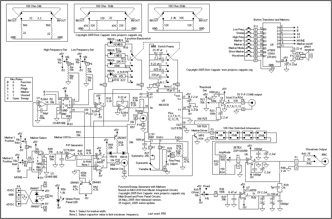
How The MAX038 Works :
======================
Surprisingly, the MAX038 does not use any fancy or patented circuit
techniques to produce frequencies up to and beyond 20MHz. Instead it uses a
simple relaxation type oscillator that operates by charging and discharging a
capacitor (on pin 5) using a constant current. It is basically a dual slope
integrator that produces a triangle wave the frequency of which is determined
by the external oscillator capacitor and the input current at the Iin pin.
This internal triangle wave is fed into an internal comparator to produce the
square wave function. The sine wave function is produced by feeding the
triangle wave into a sine wave shaping circuit that automatically corrects
for the desired frequency, and produces a reasonably low distortion sine wave
at a constant amplitude.
The sine, square, and triangle waves are then fed into a multiplexer that
selects which function to output to the low impedance output buffer.
Circuit Details :
=================
The MAX038 does all of the work in generating the actual waveform, so all we
have to do is to tell it which frequency to operate at, and which type of
waveform (sine/square/triangle) to produce.
The output frequency is determined by three factors. The first one is the
value of the oscillator capacitor on pin 5, which sets the frequency range
that the chip will operate within. The second and third factors are the
Current Input "IIN" (pin 10) and the Frequency Adjust "FADJ" (pin 8) pins.
Somewhat contrary to it's name, the Frequency Adjust pin is not the best way
to adjust the output frequency. The output frequency is actually directly
proportional to the current going into the IIN pin. The FADJ input is merely
used for finer frequency adjustment (or for frequency modulation), as it only
has about 70% of the adjustment range of IIN.
The current into IIN used to adjust the output frequency can range from
approximately 2 microamps to 700 microamps. The IIN pin acts as a virtual
ground, and thus it is a simple matter of applying a positive voltage via a
resistor to IIN. This produces a current into IIN which can be simply worked
out using Ohm's law. In fact, the output frequency can be related by the
simple formula : Fo (MHz)= IIN(鍭)/Cf(pF) Where Cf is the value of the
oscillator capacitor on pin 5. This formula assumes that FADJ is at zero
volts.
The buffer circuit formed by IC2a is used to provide a stable voltage
reference to drive the current input pin IIN. This also allows use of a low
value pot (VR1) for the main frequency adjustment. An on chip 2.5V bandgap
voltage reference is fed into the voltage divider arrangement of R5, VR1, and
R6. Stopper resistors R5 and R6 stop the value of IIN from going outside of
it's allowable linear range.
Fine frequency adjustment is achieved by varying the voltage on the FADJ pin.
Unlike the IIN pin, the FADJ pin works by varying the input voltage up to
plus or minus two volts. In this circuit, the range is set to +/-1.6V by the
voltage divider action of R3, R4, and VR3. IC2b then buffers the voltage
which goes to the FADJ pin via the low pass filter of R2 and C7.
The three frequency ranges are selected by range switch S1. This simply
parallels C2 or C3 across C4 to give the low and medium ranges respectively.
For the highest range, only C4 is connected in circuit.
The Sine, Square, and Triangle functions are selected by S2. A0 (pin 3) and
A1 (pin 4) are digital select inputs which select via an internal mutiplexer,
either the Sine, Square, or triangle waveform to be fed to the output.
The digital TTL output is taken directly from the SYNC output on pin 14. This
output changes from low to high when the analog output crosses zero volts
going positive. This can be used to synchronise the analog output to some
circuit under test, however it's main use is just as a standalone TTL level
output.
The SYNC output has it's own supply pin (pin 16) that has to be decoupled
from the main analog power supply on pin 17, otherwise a small "spike" will
appear on the analog output when the digital sync output changes state. This
is why the PCB has separate power tracks running to pins 16 & 17, each with
it's own decoupling capacitor.
Output from the MAX038 is fixed at +/-1V regardless of the waveform type
selected. This output level is referenced to the chip's internal 2.5 bandgap
voltage reference. If a larger output voltage is required, then an external
amplifier will have to be added.
The MAX038 contains it's own low impedance output buffer, but this is of no
use if the final output level needs to be varied, in this case by VR2. The
wiper of VR2 is fed to the final stage buffer chip IC3, an EL2001
manufactured by Elantec. The EL2001 is a 70MHz fixed unity gain buffer
capable of driving 50?coaxial lines. R17 provides close to a standard 50?output impedance.
The power supply circuit comprising REG1 and REG2 is a standard +/- 5V
regulated supply fed by a half wave rectified AC input.
CONSTRUCTION :
==============
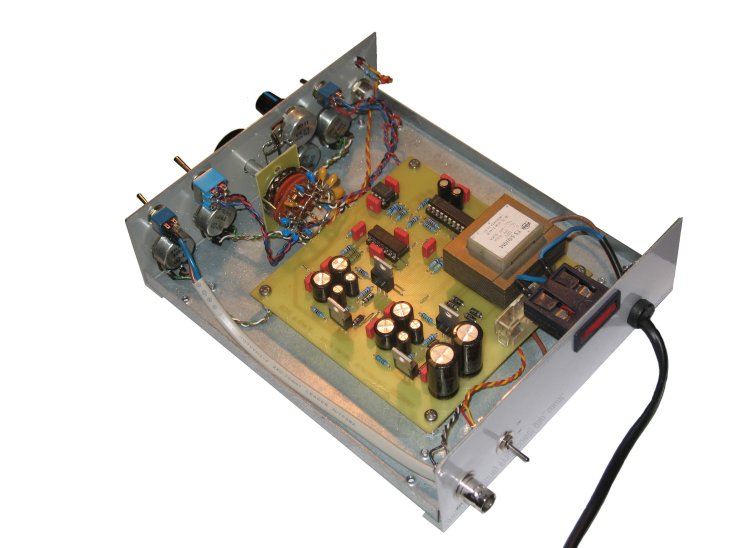
As can be seen from the photos, the unit is housed in a standard UB1 jiffy
box measuring 90 x 150 x 50mm. This allows just enough room for both the
main PCB and a small 7V AC mains transformer with an IEC mains input
connector and fuse.
All of the circuitry for the unit is contained on a single sided PCB
measuring 115 x 40mm, which is attached via the POT's to the front panel. The
only internal wiring is to and from the mains transformer, and BNC output
connectors. All of the POT's and switches are mounted at right angles along
one side of the PCB. This not only makes assembly easier, but also reduces
noise from internal wiring and provides a support for the PCB.
Start assembly with the low profile components such as the resistors and two
diodes, followed by the bypass capacitors and IC's, and then the rest of the
components. With IC1 being more expensive than most of the other components
combined, some constructors may wish to mount it in a socket. However, for
best performance it is recommended that it be soldered directly onto the PCB.
If using a socket, then ensure that it is a low profile machine pin type.
Using a 7VAC transformer for the supply, the regulators will only become warm
and should not require a heatsink for normal operation. However, if a higher
voltage AC supply is used, the regulators will most probably require a
heatsink for any sort of continuous operation. If adding a heatsink, be sure
not to short the tag's of both regulators together, as one is the supply
input and the other is ground !.
The next step is to drill the required holes in the front panel. Use a
photocopy of the drilling template provided. Make sure that the centre hole
for the pots is about 30mm in from one side of the front panel. If the PCB
is mounted to close to the middle of the box then there will be no room to
mount the transformer. There are no front panel mounting nuts used on the
switches, so make sure these holes are clean and aligned properly. Now
apply the front panel label ensuring that it is aligned with the controls.
Now turn your attention to the holes required for the IEC mains connector,
fuse holder, and transformer. The alignment of these holes is not critical,
however it is recommended to mount the components as shown in the inside shot
of the unit.
The mains wiring and transformer should be kept as far away from the PCB as
possible, to minimise hum and risk of shorting. You can add a blank piece of
earthed PCB between the transformer and PCB to divide the box into two
halves, one for the PCB and the other for the transformer and mains wiring.
If you do this, be sure to connect the blank PCB to the mains earth.
When wiring the fuse holder to the active pin of the IEC connector, make sure
it is connected to the END tag of the fuse holder and not the side tag. This
is to ensure that the fuse holder does not become live when the fuse is
replaced. Be sure to insulate all mains wiring, and make a solid mains earth
connection to the transformer chassis.
The transformer is a Dick Smith type M-2824, which is a 7V centre-tap with an
extra 7.5V winding. Only the 7V winding is used, so the centre-tap and extra
windings can be cut off. Alternatively, insulate the ends and tie them up
neatly within the case.
Before connecting power, double check all of the mains wiring and measure the
transformer primary at the IEC input pins, you should get a value of around
2K?
Before installing IC1 in it's socket, apply power and make sure that you get
+5V and -5V on pins 17 and 20 respectively.
Once you have finished construction and the power on checks, the unit should
be ready for use.
IN OPERATION :
==============
As there are no alignment or adjustment operations to perform prior to
operation, the unit should work first go as described.
Connect the output to an oscilloscope and apply power. With the level control
set to maximum, you should be able to get a waveform of the type selected by
S2. Ensure that the three types of waveform are selectable, and that the MAIN
and FINE frequency adjustment controls work on all three ranges selectable by
S1. The three frequency ranges should overlap each other, but if there is a
gap between any of the ranges, C2, C3, or C4 might not have the correct
tolerance, however this would be unlikely.
The three frequency ranges on the front panel are to be used as a guide only,
as the actual range values are determined by the tolerance of the oscillator
components. So setting the range to the "500Hz-100KHz" position and turning
the frequency controls fully in one direction will most probably NOT give the
indicated value.
The front panel frequency adjustment controls do not include a calibrated
scale, as the very wide frequency coverage of each range would make the scale
almost meaningless. This unit therefore, should be used in conjunction with a
frequency meter. A "T" piece BNC connector can be used to allow simultaneous
use of a frequency meter and the circuit to be tested.
Using an oscilloscope, there should be little or no apparent distortion of
the sine wave up to 20MHz. However, the square wave function begins to
approach a sine wave at frequencies above about 10MHz. This is due to a
bandwidth limitation of the MAX038's output buffer. The triangle wave also
suffers from this bandwidth limitation, but to a much lesser degree, and is
still usable approaching 20MHz. To get any sort of accurate picture of the
output waveform at 20MHz and above, will require the use of an oscilloscope
with a bandwidth of at least 100MHz.
Two prototype units reached a frequency of around 25MHz, with the sine wave
still being reasonably clean. The final upper frequency all depends on the
actual value of C4. C4 may be able to be tweaked to reach an upper frequency
of over 30MHz. Higher frequencies and lower distortion are possible, but
require the use of a properly laid out double sided PCB which is not
warranted in a low cost design such as this.
That's all there is to the new low cost 20MHz function generator. I'm sure
you'll find the unit as invaluable as I have. Happy generating !.
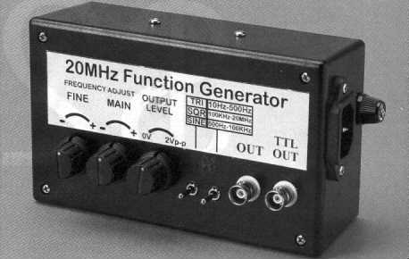
1 (原文件名:hsfg.jpg)
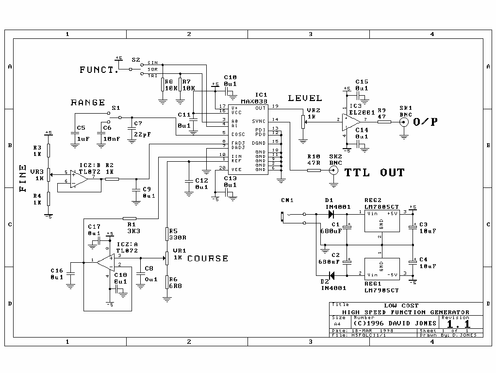
2 (原文件名:hsfglc11.gif) |
|


 发表于 2009-6-22 20:21:27