|
|
 发表于 2008-2-21 14:16:29
|
显示全部楼层
发表于 2008-2-21 14:16:29
|
显示全部楼层
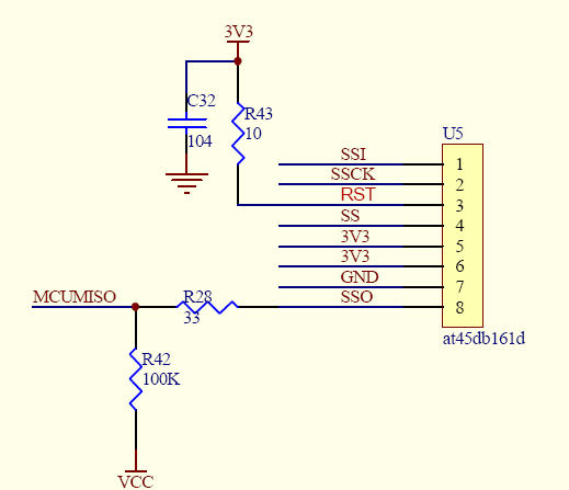
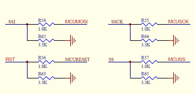
4.1测试at45DB161D
#ifndef AT45DB161D_H
#define AT45DB161D_H
#include<global.h>
#include<iom128v.h>
#include<macros.h>
#include "at45db161d_commands.h"
#ifndef SPI
#define DATAOUT 11
#define DATAIN 12
#define SPICLOCK 13
#define SLAVESELECT 10
#define RESET 8
#define WP 7
/*
#define DF_CS_inactive digitalWrite(SLAVESELECT,HIGH)
#define DF_CS_active digitalWrite(SLAVESELECT,LOW)
*/
/*
#define DF_CS_inactive PORTB|=_BV(DDB0)
#define DF_CS_active PORTB&=~_BV(DDB0)
*/
#define DF_CS_inactive PORTB|=1
#define DF_CS_active PORTB&=0xfe
#endif /* SPI */
#define READY_BUSY 0x80
#define COMPARE 0x40
#define PROTECT 0x02
#define PAGE_SIZE 0x01
#define DEVICE_DENSITY 0x2C
struct ATD45DB161D_ID
{
uint8_t manufacturer;
uint8_t device[2];
uint8_t extendedInfoLength;
};
void ATD45DB161D_Init(void);
uint8_t ReadStatusRegister(void);
void ReadManufacturerAndDeviceID(struct ATD45DB161D_ID *id);
void ReadMainMemoryPage(uint16_t page, uint16_t offset);
void ContinuousArrayRead(uint16_t page, uint16_t offset, uint8_t low);
void BufferRead(uint8_t bufferNum, uint16_t offset, uint8_t low);
void BufferWrite(uint8_t bufferNum, uint16_t offset);
void BufferToPage(uint8_t bufferNum, uint16_t page, uint8_t erase);
void PageToBuffer(uint16_t page, uint8_t bufferNum);
void PageErase(uint16_t page);
void BlockErase(uint16_t block);
void SectoreErase(uint8_t sector);
void ChipErase(void);
void BeginPageWriteThroughBuffer(uint16_t page, uint16_t offset, uint8_t bufferNum);
void EndAndWait(void);
int8_t ComparePageToBuffer(uint16_t page, uint8_t bufferNum);
void DeepPowerDown(void);
void ResumeFromDeepPowerDown(void);
#endif /* AT45DB161D_H */
#ifndef AT45DB161D_COMMANDS_H
#define AT45DB161D_COMMANDS_H
#define AT45DB161D_PAGE_READ 0xD2
#define AT45DB161D_CONTINUOUS_READ_LOW_FREQ 0x03
#define AT45DB161D_CONTINUOUS_READ_HIGH_FREQ 0x0B
#define AT45DB161D_BUFFER_1_READ_LOW_FREQ 0xD1
#define AT45DB161D_BUFFER_2_READ_LOW_FREQ 0xD3
#define AT45DB161D_BUFFER_1_READ 0xD4
#define AT45DB161D_BUFFER_2_READ 0xD6
#define AT45DB161D_BUFFER_1_WRITE 0x84
#define AT45DB161D_BUFFER_2_WRITE 0x87
#define AT45DB161D_BUFFER_1_TO_PAGE_WITH_ERASE 0x83
#define AT45DB161D_BUFFER_2_TO_PAGE_WITH_ERASE 0x86
#define AT45DB161D_BUFFER_1_TO_PAGE_WITHOUT_ERASE 0x88
#define AT45DB161D_BUFFER_2_TO_PAGE_WITHOUT_ERASE 0x89
#define AT45DB161D_PAGE_ERASE 0x81
#define AT45DB161D_BLOCK_ERASE 0x50
#define AT45DB161D_SECTOR_ERASE 0x7C
#define AT45DB161D_CHIP_ERASE_0 0xC7
#define AT45DB161D_CHIP_ERASE_1 0x94
#define AT45DB161D_CHIP_ERASE_2 0x80
#define AT45DB161D_CHIP_ERASE_3 0x9A
#define AT45DB161D_PAGE_THROUGH_BUFFER_1 0x82
#define AT45DB161D_PAGE_THROUGH_BUFFER_2 0x85
#ifdef AT45DB161D_EXPERT_MODE
/* Use the following commands at your own risk ! */
#define AT45DB161D_ENABLE_SECTOR_PROTECTION_0 0x3D
#define AT45DB161D_ENABLE_SECTOR_PROTECTION_1 0x2A
#define AT45DB161D_ENABLE_SECTOR_PROTECTION_2 0x7F
#define AT45DB161D_ENABLE_SECTOR_PROTECTION_3 0xA9
#define AT45DB161D_DISABLE_SECTOR_PROTECTION_0 0x3D
#define AT45DB161D_DISABLE_SECTOR_PROTECTION_1 0x2A
#define AT45DB161D_DISABLE_SECTOR_PROTECTION_2 0x7F
#define AT45DB161D_DISABLE_SECTOR_PROTECTION_3 0x9A
#define AT45DB161D_ERASE_SECTOR_PROTECTION_REGISTER_0 0x3D
#define AT45DB161D_ERASE_SECTOR_PROTECTION_REGISTER_0 0x2A
#define AT45DB161D_ERASE_SECTOR_PROTECTION_REGISTER_0 0x7F
#define AT45DB161D_ERASE_SECTOR_PROTECTION_REGISTER_0 0xCF
#define AT45DB161D_PROGRAM_SECTOR_PROTECTION_REGISTER_0 0x3D
#define AT45DB161D_PROGRAM_SECTOR_PROTECTION_REGISTER_1 0x2A
#define AT45DB161D_PROGRAM_SECTOR_PROTECTION_REGISTER_2 0x7F
#define AT45DB161D_PROGRAM_SECTOR_PROTECTION_REGISTER_3 0xFC
#define AT45DB161D_SECTOR_LOCKDOWN_0 0X3D
#define AT45DB161D_SECTOR_LOCKDOWN_1 0x2A
#define AT45DB161D_SECTOR_LOCKDOWN_2 0x7F
#define AT45DB161D_SECTOR_LOCKDOWN_3 0x30
#define AT45DB161D_PROGRAM_SECURITY_REGISTER_0 0x9B
#define AT45DB161D_PROGRAM_SECURITY_REGISTER_1 0x00
#define AT45DB161D_PROGRAM_SECURITY_REGISTER_2 0x00
#define AT45DB161D_PROGRAM_SECURITY_REGISTER_3 0x00
#endif /* AT45DB161D_EXPERT_MODE */
#define AT45DB161D_READ_SECTOR_PROTECTION_REGISTER 0x32
#define AT45DB161D_READ_SECTOR_LOCKDOWN_REGISTER 35H
#define AT45DB161D_READ_SECURITY_REGISTER 0x77
#define AT45DB161D_TRANSFER_PAGE_TO_BUFFER_1 0x53
#define AT45DB161D_TRANSFER_PAGE_TO_BUFFER_2 0x55
#define AT45DB161D_COMPARE_PAGE_TO_BUFFER_1 0x60
#define AT45DB161D_COMPARE_PAGE_TO_BUFFER_2 0x61
#define AT45DB161D_AUTO_PAGE_REWRITE_THROUGH_BUFFER_1 0x58
#define AT45DB161D_AUTO_PAGE_REWRITE_THROUGH_BUFFER_2 0x59
#define AT45DB161D_DEEP_POWER_DOWN 0xB9
#define AT45DB161D_RESUME_FROM_DEEP_POWER_DOWN 0xAB
#define AT45DB161D_STATUS_REGISTER_READ 0xD7
#define AT45DB161D_READ_MANUFACTURER_AND_DEVICE_ID 0x9F
#define AT45DB161D_BUFFER_1_READ_LEGACY 0X54
#define AT45DB161D_BUFFER_2_READ_LEGACY 0x56
#define AT45DB161D_PAGE_READ_LEGACY 0x52
#define AT45DB161D_CONTINUOUS_READ_LEGACY 0x68
#define AT45DB161D_STATUS_REGISTER_READ_LEGACY 0x57
#endif /* AT45DB161D_COMMANDS_H */
at45db161d.c原程序
#include "at45db161d.h"
#include<iom128v.h>
#include<macros.h>
#include<delay.h>
//#define DF_CS_inactive PORTB|=1
//#define DF_CS_active PORTB&=0xfe
uint8_t spi_transfer(uint8_t data)
{
SPDR = data;
while(!(SPSR & (1 << SPIF))) ;
return SPDR;
}
void ATD45DB161D_Init(void)
{
uint8_t clr;
/* Initialize pinout */
/*pinMode(DATAOUT, OUTPUT);
pinMode(DATAIN, INPUT);
pinMode(SPICLOCK, OUTPUT);
pinMode(SLAVESELECT, OUTPUT);
pinMode(DATAIN, INPUT);
*/
//DDRB|=(1<<DDB2)|(1<<DDB1)|(1<<DDB0);
//设置SS,SCK,MOSI为输出,MIOS为输入
DDRB&=0XF7;
DDRB|=0X07;
/* Disable device */
DF_CS_inactive;
/* Setup SPI 主机模式空闲时为高,采样结束沿采样 1/4主频率*/
SPCR = (1 << SPE) | (1 << MSTR) | (1 << CPOL) | (1 << CPHA);
/* Cleanup registers */
clr = SPSR;
clr = SPDR;
}
uint8_t ReadStatusRegister(void)
{
uint8_t status;
DF_CS_inactive; /* Make sure to toggle CS signal in order */
DF_CS_active; /* to reset Dataflash command decoder */
/* Send status read command */
spi_transfer(AT45DB161D_STATUS_REGISTER_READ);
/* Get result with a dummy write */
status = spi_transfer(0x00);
return status;
}
void ReadManufacturerAndDeviceID(struct ATD45DB161D_ID *id)
{
DF_CS_inactive; /* Make sure to toggle CS signal in order */
DF_CS_active; /* to reset Dataflash command decoder */
/* Send status read command */
spi_transfer(AT45DB161D_READ_MANUFACTURER_AND_DEVICE_ID);
/* Manufacturer ID */
id->manufacturer = spi_transfer(0xff);
/* Device ID (part 1) */
id->device[0] = spi_transfer(0xff);
/* Device ID (part 2) */
id->device[1] = spi_transfer(0xff);
/* Extended Device Information String Length */
id->extendedInfoLength = spi_transfer(0xff);
}
void ReadMainMemoryPage(uint16_t page, uint16_t offset)
{
DF_CS_inactive; /* Make sure to toggle CS signal in order */
DF_CS_active; /* to reset Dataflash command decoder */
/* Send opcode */
spi_transfer(AT45DB161D_PAGE_READ);
/* Address (page | offset) */
spi_transfer((uint8_t)(page >> 6));
spi_transfer((uint8_t)((page << 2) | (offset >> 8)));
spi_transfer((uint8_t)(offset & 0xff));
/* 4 "don't care" bytes */
spi_transfer(0x00);
spi_transfer(0x00);
spi_transfer(0x00);
spi_transfer(0x00);
}
void ContinuousArrayRead(uint16_t page, uint16_t offset, uint8_t low)
{
DF_CS_inactive; /* Make sure to toggle CS signal in order */
DF_CS_active; /* to reset Dataflash command decoder */
/* Send opcode */
spi_transfer( low ? AT45DB161D_CONTINUOUS_READ_LOW_FREQ :
AT45DB161D_CONTINUOUS_READ_HIGH_FREQ );
/* Address (page | offset) */
spi_transfer((uint8_t)(page >> 6));
spi_transfer((uint8_t)((page << 2) | (offset >> 8)));
spi_transfer((uint8_t)(offset & 0xff));
}
void BufferRead(uint8_t bufferNum, uint16_t offset, uint8_t low)
{
DF_CS_inactive; /* Make sure to toggle CS signal in order */
DF_CS_active; /* to reset Dataflash command decoder */
/* Send opcode */
if(bufferNum == 1)
{
spi_transfer(low ? AT45DB161D_BUFFER_1_READ_LOW_FREQ :
AT45DB161D_BUFFER_1_READ);
}
else
{
spi_transfer(low ? AT45DB161D_BUFFER_2_READ_LOW_FREQ :
AT45DB161D_BUFFER_2_READ);
}
/* 14 "Don't care" bits */
spi_transfer(0x00);
/* Rest of the "don't care" bits + bits 8,9 of the offset */
spi_transfer((uint8_t)(offset >> 8));
/* bits 7-0 of the offset */
spi_transfer((uint8_t)(offset & 0xff));
}
void BufferWrite(uint8_t bufferNum, uint16_t offset)
{
DF_CS_inactive; /* Make sure to toggle CS signal in order */
DF_CS_active; /* to reset Dataflash command decoder */
spi_transfer( (bufferNum == 1) ? AT45DB161D_BUFFER_1_WRITE :
AT45DB161D_BUFFER_2_WRITE);
/* 14 "Don't care" bits */
spi_transfer(0x00);
/* Rest of the "don't care" bits + bits 8,9 of the offset */
spi_transfer((uint8_t)(offset >> 8));
/* bits 7-0 of the offset */
spi_transfer((uint8_t)(offset & 0xff));
}
void BufferToPage(uint8_t bufferNum, uint16_t page, uint8_t erase)
{
DF_CS_inactive; /* Make sure to toggle CS signal in order */
DF_CS_active; /* to reset Dataflash command decoder */
/* Opcode */
if(erase)
{
spi_transfer( (bufferNum == 1) ? AT45DB161D_BUFFER_1_TO_PAGE_WITH_ERASE :
AT45DB161D_BUFFER_2_TO_PAGE_WITH_ERASE);
}
else
{
spi_transfer( (bufferNum == 1) ? AT45DB161D_BUFFER_1_TO_PAGE_WITHOUT_ERASE :
AT45DB161D_BUFFER_2_TO_PAGE_WITHOUT_ERASE);
}
/*
* 3 address bytes consist of :
* - 2 don’t care bits
* - 12 page address bits (PA11 - PA0) that specify the page in
* the main memory to be written
* - 10 don’t care bits
*/
spi_transfer((uint8_t)(page >> 6));
spi_transfer((uint8_t)(page << 2));
spi_transfer(0x00);
DF_CS_inactive; /* Start transfer */
DF_CS_active; /* If erase was set, the page will first be erased */
/* Wait for the end of the transfer */
while(!(ReadStatusRegister() & READY_BUSY))
{}
}
void PageToBuffer(uint16_t page, uint8_t bufferNum)
{
DF_CS_inactive; /* Make sure to toggle CS signal in order */
DF_CS_active; /* to reset Dataflash command decoder */
/* Send opcode */
spi_transfer((bufferNum == 1) ? AT45DB161D_TRANSFER_PAGE_TO_BUFFER_1 :
AT45DB161D_TRANSFER_PAGE_TO_BUFFER_2);
/*
* 3 address bytes consist of :
* - 2 don’t care bits
* - 12 page address bits (PA11 - PA0) that specify the page in
* the main memory to be written
* - 10 don’t care bits
*/
spi_transfer((uint8_t)(page >> 6));
spi_transfer((uint8_t)(page << 2));
spi_transfer(0x00);
DF_CS_inactive; /* Start page transfer */
DF_CS_active;
/* Wait for the end of the transfer */
while(!(ReadStatusRegister() & READY_BUSY))
{}
}
void PageErase(uint16_t page)
{
DF_CS_inactive; /* Make sure to toggle CS signal in order */
DF_CS_active; /* to reset Dataflash command decoder */
/* Send opcode */
spi_transfer(AT45DB161D_PAGE_ERASE);
/*
* 3 address bytes consist of :
* - 2 don’t care bits
* - 12 page address bits (PA11 - PA0) that specify the page in
* the main memory to be written
* - 10 don’t care bits
*/
spi_transfer((uint8_t)(page >> 6));
spi_transfer((uint8_t)(page << 2));
spi_transfer(0x00);
DF_CS_inactive; /* Start block erase */
DF_CS_active;
/* Wait for the end of the block erase operation */
while(!(ReadStatusRegister() & READY_BUSY))
{}
}
void BlockErase(uint16_t block)
{
DF_CS_inactive; /* Make sure to toggle CS signal in order */
DF_CS_active; /* to reset Dataflash command decoder */
/* Send opcode */
spi_transfer(AT45DB161D_BLOCK_ERASE);
/*
* 3 address bytes consist of :
* - 2 don’t care bits
* - 9 block address bits (PA11 - PA3)
* - 13 don’t care bits
*/
spi_transfer((uint8_t)(block >> 3));
spi_transfer((uint8_t)(block << 5));
spi_transfer(0x00);
DF_CS_inactive; /* Start block erase */
DF_CS_active;
/* Wait for the end of the block erase operation */
while(!(ReadStatusRegister() & READY_BUSY))
{}
}
void SectoreErase(uint8_t sector)
{
DF_CS_inactive; /* Make sure to toggle CS signal in order */
DF_CS_active; /* to reset Dataflash command decoder */
/* Send opcode */
spi_transfer(AT45DB161D_SECTOR_ERASE);
/*
* 3 address bytes consist of :
*/
if((sector == 0x0a) || (sector == 0x0b))
{
/*
* - 11 don’t care bits
* -
* - 12 don’t care bits
*/
spi_transfer(0x00);
spi_transfer(((sector & 0x01) << 4));
spi_transfer(0x00);
}
else
{
/*
* - 2 don't care bits
* - 4 sector number bits
* - 18 don't care bits
*/
spi_transfer(sector << 1);
spi_transfer(0x00);
spi_transfer(0x00);
}
DF_CS_inactive; /* Start block erase */
DF_CS_active;
/* Wait for the end of the block erase operation */
while(!(ReadStatusRegister() & READY_BUSY))
{}
}
void ChipErase(void)
{
DF_CS_inactive; /* Make sure to toggle CS signal in order */
DF_CS_active; /* to reset Dataflash command decoder */
/* Send chip erase sequence */
spi_transfer(AT45DB161D_CHIP_ERASE_0);
spi_transfer(AT45DB161D_CHIP_ERASE_1);
spi_transfer(AT45DB161D_CHIP_ERASE_2);
spi_transfer(AT45DB161D_CHIP_ERASE_3);
DF_CS_inactive; /* Start chip erase */
DF_CS_active;
/* Wait for the end of the chip erase operation */
while(!(ReadStatusRegister() & READY_BUSY))
{}
}
void BeginPageWriteThroughBuffer(uint16_t page, uint16_t offset, uint8_t bufferNum)
{
DF_CS_inactive; /* Make sure to toggle CS signal in order */
DF_CS_active; /* to reset Dataflash command decoder */
/* Send opcode */
spi_transfer((bufferNum == 1) ? AT45DB161D_PAGE_THROUGH_BUFFER_1 :
AT45DB161D_PAGE_THROUGH_BUFFER_2);
/* Address */
spi_transfer((uint8_t)(page >> 6));
spi_transfer((uint8_t)((page << 2) | (offset >> 8)));
spi_transfer((uint8_t)offset);
}
void EndAndWait(void)
{
DF_CS_inactive; /* End current operation */
DF_CS_active; /* Some internal operation may occur
* (buffer to page transfer, page erase, etc... ) */
/* Wait for the chip to be ready */
while(!(ReadStatusRegister() & READY_BUSY))
{}
}
int8_t ComparePageToBuffer(uint16_t page, uint8_t bufferNum)
{
uint8_t status;
DF_CS_inactive; /* Make sure to toggle CS signal in order */
DF_CS_active; /* to reset Dataflash command decoder */
/* Send opcode */
spi_transfer((bufferNum == 1) ? AT45DB161D_COMPARE_PAGE_TO_BUFFER_1 :
AT45DB161D_COMPARE_PAGE_TO_BUFFER_2);
/* Page address */
spi_transfer((uint8_t)(page >> 6));
spi_transfer((uint8_t)(page << 2));
spi_transfer(0x00);
DF_CS_inactive; /* Start comparaison */
DF_CS_active;
/* Wait for the end of the comparaison and get the result */
while(!((status = ReadStatusRegister()) & READY_BUSY))
{}
return ((status & COMPARE) == COMPARE);
}
void DeepPowerDown(void)
{
DF_CS_inactive; /* Make sure to toggle CS signal in order */
DF_CS_active; /* to reset Dataflash command decoder */
/* Send opcode */
spi_transfer(AT45DB161D_DEEP_POWER_DOWN);
/* Enter Deep Power-Down mode */
DF_CS_inactive;
/* Safety delay */
delay_ms(100);
}
void ResumeFromDeepPowerDown(void)
{
DF_CS_inactive; /* Make sure to toggle CS signal in order */
DF_CS_active; /* to reset Dataflash command decoder */
/* Send opcode */
spi_transfer(AT45DB161D_RESUME_FROM_DEEP_POWER_DOWN);
/* Resume device */
DF_CS_inactive;
/* The CS pin must stay high during t_RDPD microseconds before the device
* can receive any commands.
* On the at45db161D t_RDPD = 35 microseconds. But we will wait 100
* (just to be sure). */
delay_ms(100);
}
测试程序1
void ATD45DB161D_test(void)
{
struct ATD45DB161D_ID *id1;
sendstring1("now test ATD45DB161D dataflash !\n");
sendstring1("1.ReadStatusRegister\n");
// sendchar1(char2hex(ReadStatusRegister()));
sendinthex1(ReadStatusRegister());
sendstring1("\n");
sendstring1("2. ReadManufacturerAndDeviceID\n");
ReadManufacturerAndDeviceID(id1);
/* Manufacturer ID */
sendstring1("id1->manufacturer=");
// sendchar1(char2hex(id1->manufacturer));
sendinthex1(id1->manufacturer);
sendstring1("\n");
/* Device ID (part 1) */
sendstring1("id1->device[0]=");
//sendchar1(char2hex(id1->device[0]));
sendinthex1(id1->device[0]);
sendstring1("\n");
/* Device ID (part 2) */
sendstring1("id1->device[1]=");
//sendchar1(char2hex(id1->device[1]));
sendinthex1(id1->device[1]);
sendstring1("\n");
/* Extended Device Information String Length */
sendstring1("id1->extendedInfoLength=");
//sendchar1(char2hex(id1->extendedInfoLength));
sendinthex1(id1->extendedInfoLength);
sendstring1("\n");
sendstring1("3. ChipErase test\n");
sendstring1("now ChipErase begin\n");
ChipErase();
sendstring1("now ChipErase end\n");
}
这个是串口的输出
1
1 |
|


 楼主
楼主