|
|

楼主 |
发表于 2012-1-10 14:38:02
|
显示全部楼层
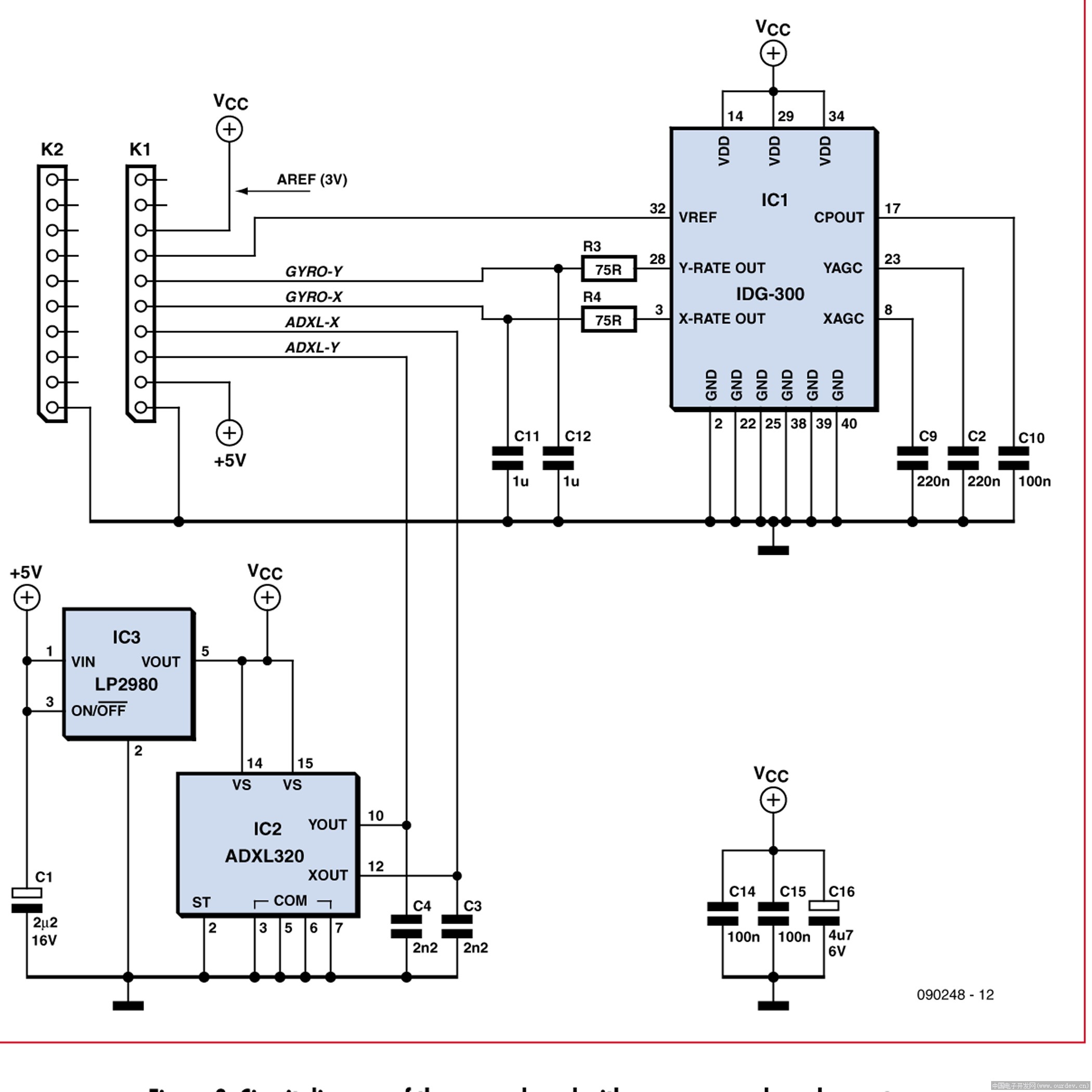
Integrated Dual-Axis Gyro
IDG-300
InvenSense, Inc., 3150A Coronado Drive, Santa Clara, CA 95054 U.S.A. 1 DOC-00075-01, 2222006
Tel: +1 (408) 988-7339 Fax: +1 (408) 988-8104 PROPRIETARY INFORMATION
Website: http//www.invensense.com ©2006 InvenSense, Inc. All rights reserved.
FEATURES
• Integrated X- and Y-axis gyro on a single chip
• Factory trimmed full scale range of ±500°/sec
• Integrated low-pass filters
• Superior vibration rejection over a wide
frequency range
• High cross-axis isolation by design
• 3V single supply operation
• 5000 g shock tolerance
• RoHS compliant (completely lead free)
• 6 x 6 x 1.5mm QFN package
APPLICATIONS
• Inertial measurement units (IMUs)
• Handheld GPS navigation devices
• Radio controlled helicopters
• Toys and game consoles
• Robotic and power tools
• Antenna positioning
• Remote control
GENERAL DESCRIPTION
The IDG-300 is an integrated dual-axis angular rate
sensor (gyroscope). It uses InvenSense’s proprietary and
patented MEMS technology with vertically driven,
vibrating masses to make a functionally complete, lowcost,
dual-axis angular rate sensor. All required
electronics are integrated onto a single chip with the
sensor.
The IDG-300 gyro uses two sensor elements with novel
vibrating dual-mass bulk silicon configurations that sense
the rate of rotation about the X- and Y-axis (in-plane
sensing). This results in a unique, integrated dual-axis
gyro with guaranteed-by-design vibration rejection and
high cross-axis isolation. It is specifically designed for
demanding consumer applications requiring low cost,
small size and high performance.
The IDG-300 gyro includes integrated electronics
necessary for application-ready functionality. It
incorporates X- and Y-axis low-pass filters and an
EEPROM for on-chip factory calibration of the sensor.
Factory trimmed scale factors eliminate the need for
external active components and end-user calibration.
This product is lead-free and Green Compliant.
VREF
32
Supply *
29
14
0.22μF
XAGC 8
0.22μF
YAGC 23 28
IDG-300
0.1μF
Reference
EEPROM
TRIM
Gain
Oscillator Demodulator
Oscillator Demodulator
Coriolis
Sense
Low-Pass
Filter
Low-Pass
Filter
Y-Rate
Sensor
X-Rate
Sensor
VDD
3
Coriolis
Sense
Charge Pump
Regulator
CPOUT GND
2 22 25 38 39 40
0.1μF/25V
17
Gain
34
Y-RATE OUT
RLPX
CLPX
Optional External
Low Pass Filter
X-RATE OUT
Optional External
Low Pass Filter
RLPY CLPy
* See Design Notes: Section 5
±10%
±10%
±20%
IDG-300
InvenSense, Inc., 3150A Coronado Drive, Santa Clara, CA 95054 U.S.A. 2 DOC-00075-01, 2222006
Tel: +1 (408) 988-7339 Fax: +1 (408) 988-8104 PROPRIETARY INFORMATION
Website: http//www.invensense.com ©2006 InvenSense, Inc. All rights reserved.
SPECIFICATIONS
All parameters specified are @ VDD=3.0 V and T=25°C. External LPF @ 2kHz. All specifications apply to both axes.
Parameters Conditions Min Typical Max Unit
SENSITIVITY
Full-Scale Range
Sensitivity
Initial Calibration Tolerance
Over Specified Temperature
Nonlinearity
Cross-axis Sensitivity
Best Fit Straight Line
-5
±500
2.0
±10
<1
±2
+5
°/s
mV/°/s
%
%
% of FS
%
ZERO-RATE OUTPUT
Static Output (Bias)
Initial Calibration Tolerance
Over Specified Temperature
-100
-300
1.5
+100
+300
V
mV
mV
FREQUENCY RESPONSE
High Frequency Cutoff
LPF Phase Delay
Internal LPF -90°
10Hz
140
-4.5
Hz
°
MECHANICAL FREQUENCIES
Resonant Frequency
Resonant Frequency
Frequency Separation
X-Axis Gyroscope
Y-Axis Gyroscope
X and Y Gyroscopes
10
13
12
15
3
14
17
kHz
kHz
kHz
OUTPUT DRIVE CAPABILITY
Output Voltage Swing
Capacitive Load Drive
Output Impedance
Load = 100kΩ to Vdd/2
0.05
100
100
Vdd-0.05
V
pF
Ω
REFERENCE
Voltage Value
Load Drive
Capacitive Load Drive
Power Supply Rejection
Over Specified Temperature
Load directly connected to VREF
VDD= 3.0V to 3.3V
1.23
1
100
1
±5
V
mA
pF
mV/V
mV
POWER-UP RESPONSE
Zero-rate settling time
To ±3°/sec
200
ms
NOISE PERFORMANCE
Rate Noise Density 0.014 °/s/√Hz
POWER SUPPLY
Operating Voltage Range
Quiescent Supply Current
Over Specified Temperature
3.0
±2
3.3
9.5
V
mA
mA
TEMPERATURE RANGE
Specified Temperature Range
Extended Temperature Range
Performance parameters are not applicable
beyond Specified Temperature Range
0 to +70
-20 to +85
°C
°C
Reference Application Diagram
IDG-300
InvenSense, Inc., 3150A Coronado Drive, Santa Clara, CA 95054 U.S.A. 3 DOC-00075-01, 2222006
Tel: +1 (408) 988-7339 Fax: +1 (408) 988-8104 PROPRIETARY INFORMATION
Website: http//www.invensense.com ©2006 InvenSense, Inc. All rights reserved.
ABSOLUTE MAXIMUM RATINGS
Stress above those listed as “Absolute Maximum Ratings” may cause permanent damage to the device. This is a stress
rating only and functional operation of the device under these conditions is not implied. Exposure to absolute maximum
rating conditions for extended periods may affect device reliability.
Parameter Rating
Supply Voltage -0.3V to +6.0V
Acceleration (Any Axis, unpowered) 5000g for 0.3ms
Operating Temperature Range -40 to +105°C
Storage Temperature Range -40 to +125°C
PACKAGE DIMENSIONS (all dimensions in mm)
b
A
A1
A3
0.10C
SEATING
PLANE
C
0.10 C B A
TOP VIEW BOTTOM VIEW
SIDE VIEW
Common
Dimensions Millimeter Dimensions Inch
S
Y
M
B
O
L Min Nom Max Min Nom Max
A 1.30 1.40 1.50 0.051 0.055 0.059
A1 0.00 0.02 0.05 0.00 0.001 0.002
A3 0.20 BSC 0.008 BSC
b 0.18 0.25 0.30 0.007 0.010 0.012
D 5.925 6.00 6.075 0.233 0.236 0.239
E 5.925 6.00 6.075 0.233 0.236 0.239
e 0.50 BSC 0.020 BSC
L 0.35 0.40 0.45 0.014 0.016 0.239
L1 0.03 0.09 0.15 0.002 0.004 0.006
D2 4.50 4.65 4.80 0.177 0.183 0.189
E2 4.50 4.65 4.80 0.177 0.183 0.189
L1
20 11
L
10
E2
D2
D2/2 40 31
30
21
E2/2
1
e
D
E
B
A
PIN #1
IDG-300
InvenSense, Inc., 3150A Coronado Drive, Santa Clara, CA 95054 U.S.A. 4 DOC-00075-01, 2222006
Tel: +1 (408) 988-7339 Fax: +1 (408) 988-8104 PROPRIETARY INFORMATION
Website: http//www.invensense.com ©2006 InvenSense, Inc. All rights reserved.
PIN DESCRIPTION
Number Pin Description
2, 22, 25, 38, 39, 40 GND Ground
14, 29, 34 VDD Positive supply voltage: +3.0V to +3.3V
3 X-Rate Out X-Rate Out
8 XAGC Amplitude control filter (See Design Notes: Section 2)
17 CPOUT Charge pump capacitor
23 YAGC Amplitude control filter (See Design Notes: Section 2)
28 Y-Rate Out Y-Rate Out
32 VREF 1.23V precision reference output
1, 9, 10,11, 12, 13,
15,16, 18, 19, 20,
21, 30, 31, 33,
35, 36, 37
RESV Reserved. Do not connect. Used for factory trimming
4 ,5, 6, 7, 24, 26, 27 NC Not internally connected; may be used for PCB routing
PIN CONNECTION (TOP VIEW) RATE SENSITIVE AXIS
This is a dual-axis rate sensing device. It produces a
positive output voltage for rotation about the X- or Y-axis,
as shown in the figure below.
VREF
RESV
RESV
GND
GND
GND
RESV
RESV
VDD
RESV
1
2
3
4
5
6
7
8
9
10
30
29
28
27
26
25
24
23
22
21
RESV
GND
X-Rate Out
NC
RESV
NC
NC
NC
XAGC
RESV
RESV
IDG-300
RESV
RESV
VDD
RESV
RESV
CPOUT
RESV
RESV
RESV
RESV
GND
YAGC
NC
GND
NC
NC
VDD
RESV
11 12 13 14 15 16 17 18 19 20
40 39 38 37 36 35 34 33 32 31
Y-Rate Out
RATEOUT
RATE IN
GND
1.23V
VDD = 3V
0.23V
2.23V
IDG-300
+
+ X
Y
40 pin QFN Package
6 x 6 x 1.5mm
IDG-300
InvenSense, Inc., 3150A Coronado Drive, Santa Clara, CA 95054 U.S.A. 5 DOC-00075-01, 2222006
Tel: +1 (408) 988-7339 Fax: +1 (408) 988-8104 PROPRIETARY INFORMATION
Website: http//www.invensense.com ©2006 InvenSense, Inc. All rights reserved.
DESIGN NOTES
1. Overview
The IDG-300 gyro is a dual-axis gyroscope consisting of
two independent vibratory MEMS gyroscopes. One
detects rotation about the X-axis; the other detects
rotation about the Y-axis. Each structure is fabricated
using InvenSense’s proprietary bulk silicon technology.
The structures are covered and hermetically sealed at the
wafer-level. The cover shields the gyro from EMI.
The gyroscope’s proof-masses are electrostatically
oscillated at resonance. An internal automatic gain
control circuit precisely sets the oscillation of the proof
masses. When the sensor is rotated about the X- or Yaxis,
the Coriolis effect causes a vibration that can be
detected by a capacitive pickoff. The resulting signal is
amplified, demodulated, and filtered to produce an analog
voltage that is proportional to the angular rate.
2. Amplitude Control
The scale factor of the gyroscope depends on the
amplitude of the mechanical motion and the trim setting
of the internal programmable gain stages. The oscillation
circuit precisely controls the amplitude to maintain
constant sensitivity over the temperature range. The
capacitors (0.22μF, ±10%) connected to Pin 8 (XAGC)
and Pin 23 (YAGC) are compensation capacitors for the
amplitude control loops.
5. Power Supply Filtering
The IDG-300 gyro should be isolated from system power
supply noise by a combination of an RC filter that
attenuates high frequency noise and a Low Drop Out
power supply regulator (LDO) that attenuates low
frequency noise. Figure below shows a typical
configuration.
The low-pass RC filter should be chosen such that it
provides significant attenuation of system noise at high
frequencies. The LDO should be a low noise regulator
(<100μV/rtHz) that exhibits good noise rejection at low
frequencies.
6. VREF
VREF is a temperature independent voltage reference
that can be used as a reference for an ADC. There is
offset between the zero rate output and VREF.
29
1.0μF
2.2Ω 0.1μF
VIN
En GND
VOUT
IDG-300
LDO
14
34
3. External Low-Pass Filter
An external low-pass filter is recommended to attenuate
high-frequency noise. The cutoff frequency should be less
than 2 kHz to attenuate tones above 10 kHz generated by
the vibrating proof-masses. Recommended RC values for
the 2 kHz filter are RLPX/RLPY and CLPX/CLPY are 750Ω and
0.1μF respectively. The sensor bandwidth is limited to 140
Hz by the internal low-pass filter. Applications that require
lower bandwidth should choose an external filter with a
cutoff frequency less than 140Hz.
4. Scale Factor
The IDG-300 Rate-Out is not ratiometric to the supply
voltage. The scale factor is calibrated at the factory and is
nominally independent of supply voltage.
Supply
IDG-300
InvenSense, Inc., 3150A Coronado Drive, Santa Clara, CA 95054 U.S.A. 6 DOC-00075-01, 2222006
Tel: +1 (408) 988-7339 Fax: +1 (408) 988-8104 PROPRIETARY INFORMATION
Website: http//www.invensense.com ©2006 InvenSense, Inc. All rights reserved.
This information furnished by InvenSense is believed to be accurate and reliable. However, no responsibility is assumed by
InvenSense for its use, or for any infringements or patents or other rights of third parties that may result from its use.
Specifications are subject to change without notice. Certain intellectual property owned by InvenSense and described in this
document is patent protected. No license is granted by implication or otherwise under any patent or patent rights of
InvenSense. This publication supersedes and replaces all information previously supplied. Trademarks that are registered
trademarks are the property of their respective companies. InvenSense products are not authorized for use as critical
components in life support devices or systems without express written approval of InvenSense.
©2006 InvenSense, Inc. All rights reserved. |
|


 发表于 2012-1-9 15:30:44